Logic Design
see https://dlcc.notion.site/fd1e2a787b11464896f55d9684337246
Ch11 Latches and Flip-flops
flip-flop: only response to a ==clock input== (but not a data input)
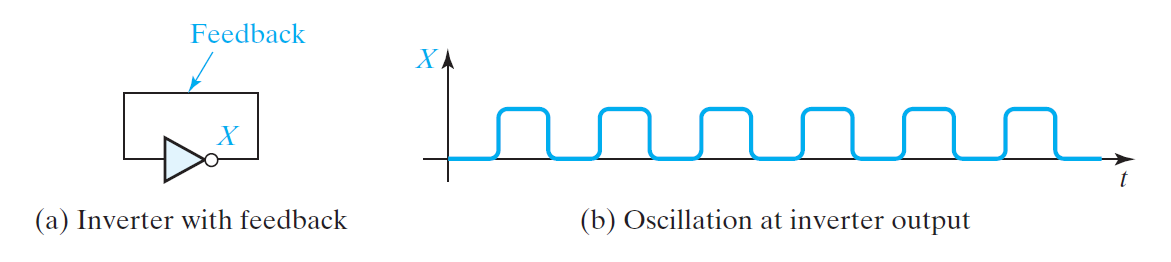
bc propagation odd number of inverters → oscillate
11.2 S-R Latch
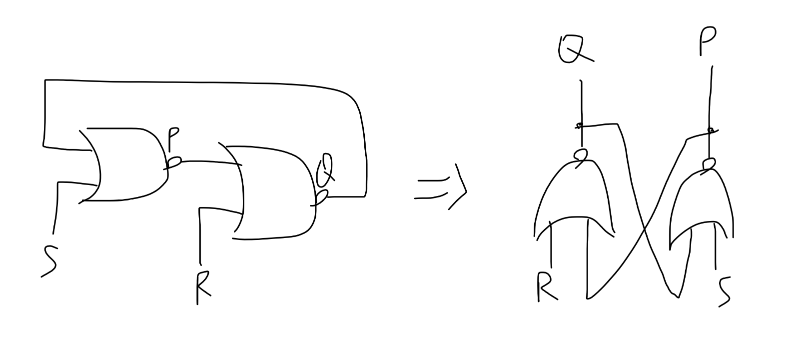
original NOR S-R Latch
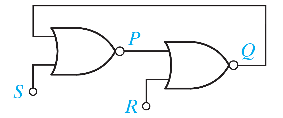 左上 → switch S → 右上 → switch S → 左下 → switch R → 右下
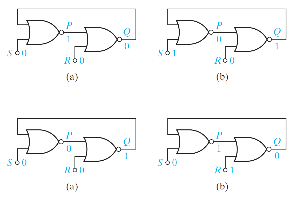
if !(S=R=1) then P == Q'
if S=R=1
when S,R=1→0
P,Q oscillate 0→1→0→1→....
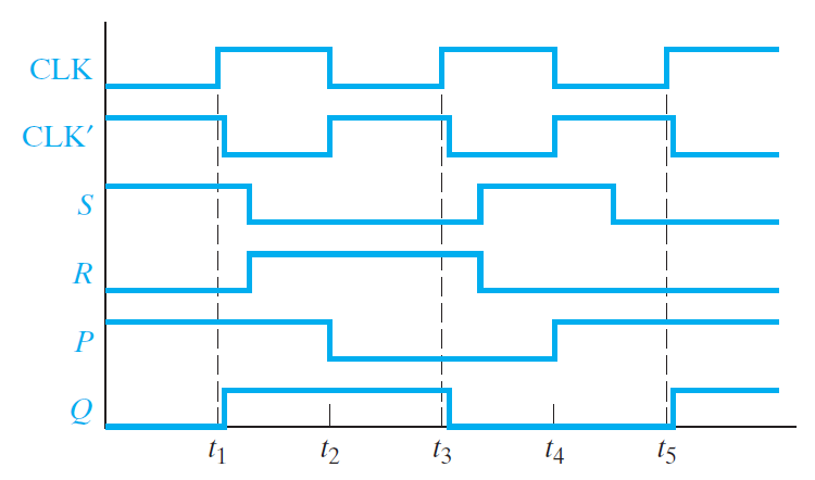
time diagram
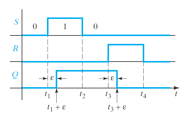
if S's or R's duration of S < ε
then Q won't change
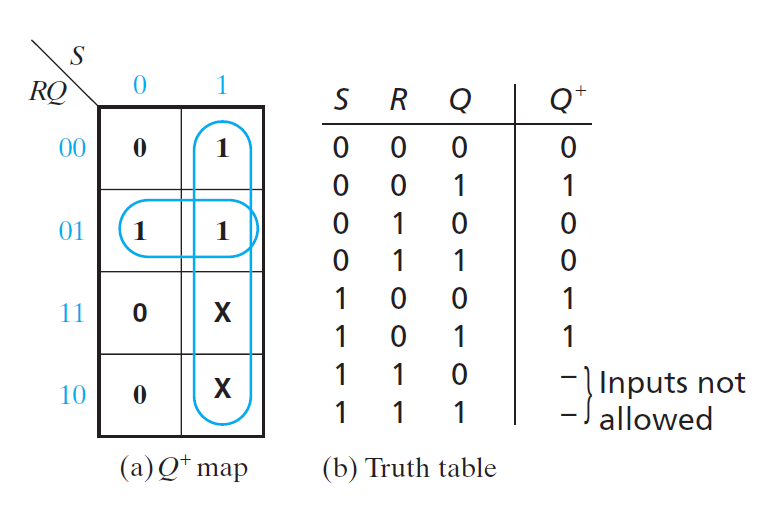
Q+ = ((Q+S)'+R)' = (Q+S)R' = R'S + R'Q P = (S+Q)' = S'Q' bc S=R=1 is disallowed (i.e. SR=0) so
==Q+= S + R'Q==
(Q+=R'S + R'Q + RS)
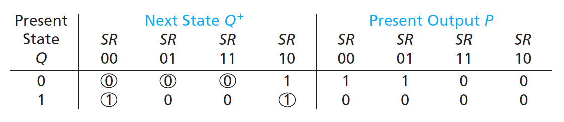
Q+=1 when
debounce switch
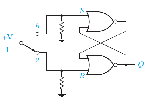
S bounces when switch to b
R bounces when switch to a
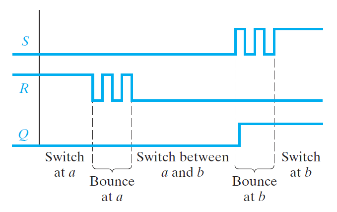
Q+=S+R'Q
Bounce at a: S=Q=0 so always 0
Bounce at b: S duration > ε let Q→1, then stays at 1 bc R=0
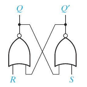
NAND S-R Latch
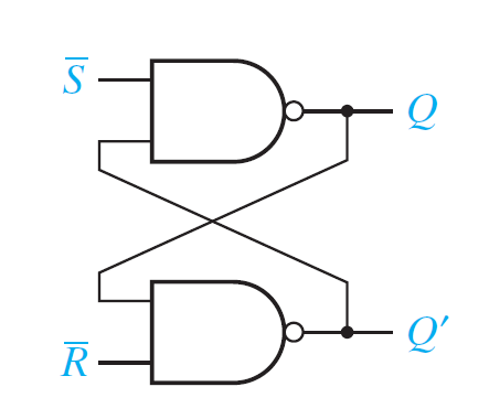
Q+ = ((QR)'S)' = QR + S'
→ = NOR S'-R' Latch
note that ==S, R switch place==
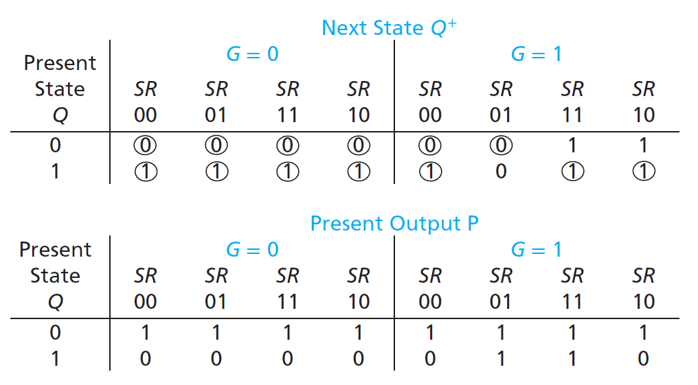
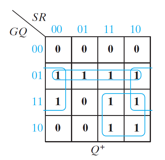
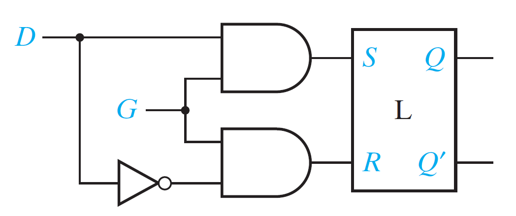
11.3 Gated Latches
NAND-gate gated S-R Latch
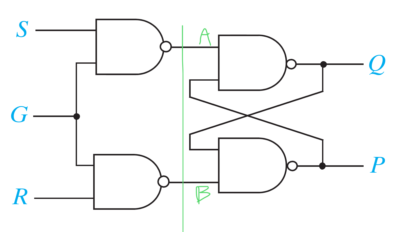
Q+ = A' + BQ = SG + (RG)'Q = SG + Q(R' + G')
P = (BQ)' = Q' + RG
when G=0, Q+=Q, P=Q' → stable
when G=1, Q+=S+QR', P=RG → original NOR S-R Latch
when S=R=1 and G=1→0
propogation time race
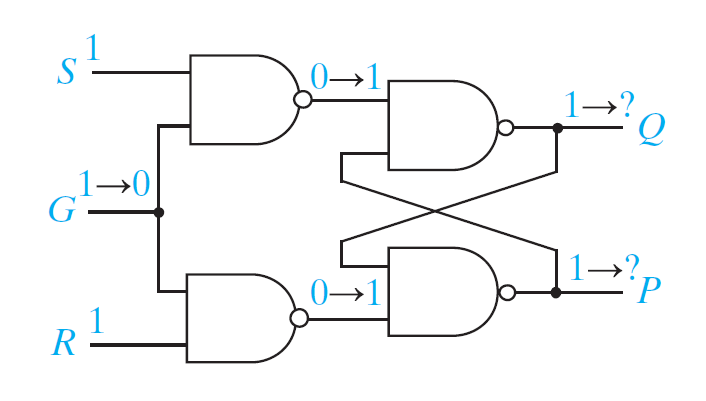
Q+=SG+Q(R'+G'):
static-1 hazard between G=0,1
1's, 0's catching problem
S=R=0, G=1, Q=0
S has a 1 glitch → Q=0→1
→ 1's catching problem
NOR S-R Latch has a 0's catching problem
so S, R inputs must not have glitch
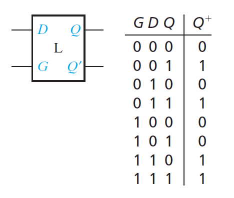
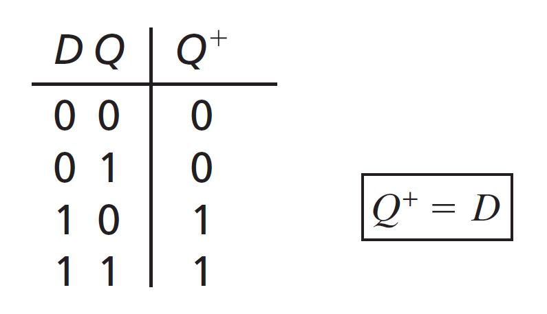
Gated D Latch
S = D, R = D'
(L 是 NOR S-R latch)
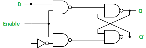
when G=0, Q+ = Q
when G=1, Q+ = S+QR = D
→transparent latch
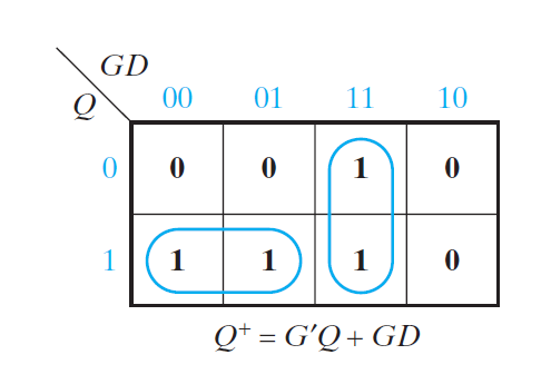
 Q+ = G'Q + GD
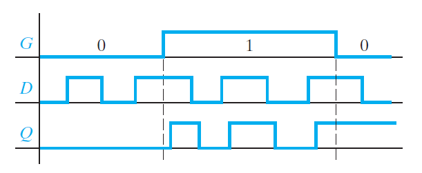
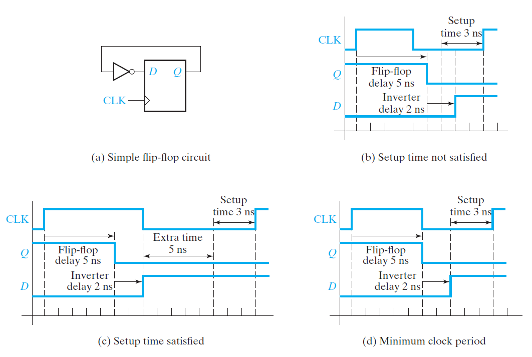
when Clk=1 and x=1, D oscillates
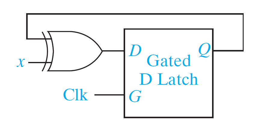
opening a clock for only a little time (let D pass to Q but not Q→Q' pass to D) will solve the problem
so we restrict the flip-flop to only change on the edge of the clock (input change → no effect)
→ edge-triggered flip-flop
11.4 Edge-Triggered D Flip-Flop
rising-edge trigger(left): output change when Clk=0→1
falling-edge trigger(right, has bubble): output change when Clk=1→0
falling-edge triggered D flip-flop time diagram
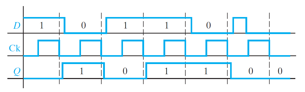
when Clk=1→0, Q = D the moment Clk change→
rising edge triggered D flip-flop
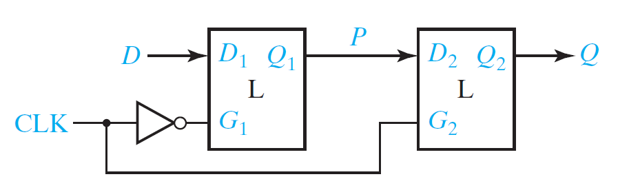
when Clk=0, D pass to P, Q+=Q
when Clk=0→1, D pass to P pass to Q
when Clk=1, Q hold the D when Clk 0→1, D now doesn't affect anything
when Clk=0→1, nothing happens
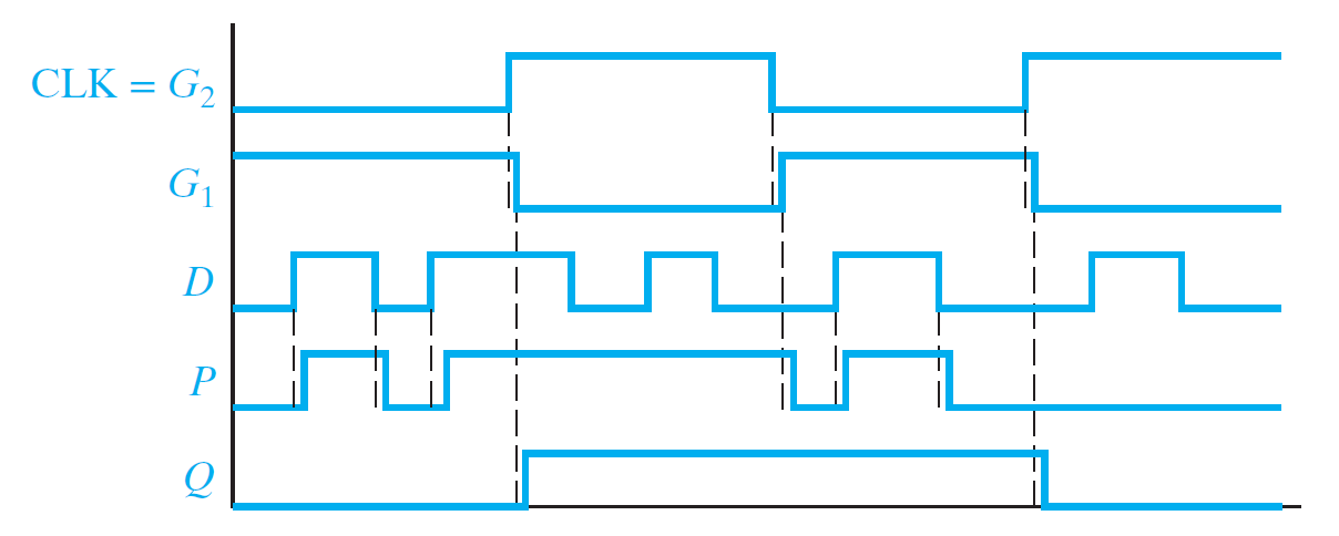
tsu (setup time) = D's must-stable time before Clk 0→1
th (hold time) = D's must=stable time after Clk 0→1
tp = clock's propagational delay
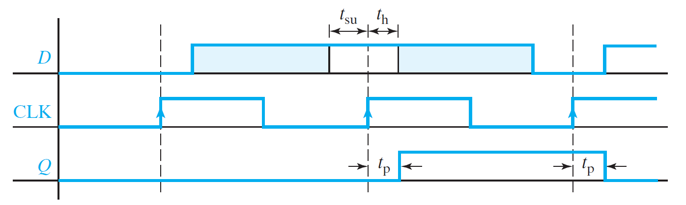
an example of minumum clock period
11.5 S-R Flip-Flop
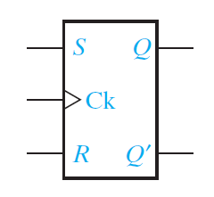
(rising-edge)
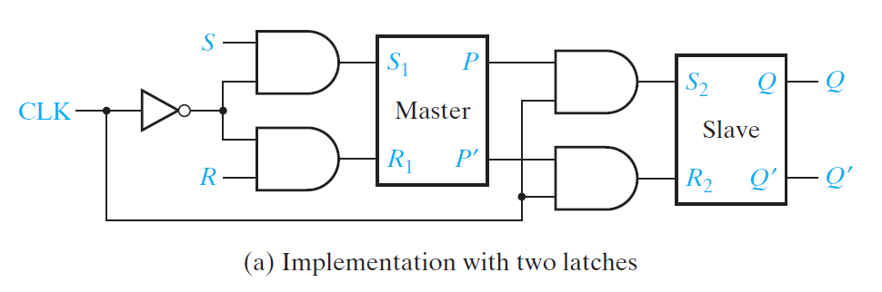
NOR-gate S-R latch: Q+=S+R'Q
when Clk=0, S1=S, R1=R (Master)
when Clk=1, Q=P
Q change when Clk=0→1
at t4, Clk=1→0, so P=S+R'Q=1
at t4, Clk=0→1, so P=1 pass to Q
but S=R=0 then, Q shoudln't change
so we ==only allow inputs change when clock is high==
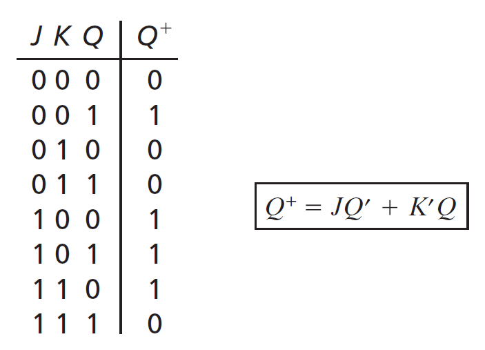
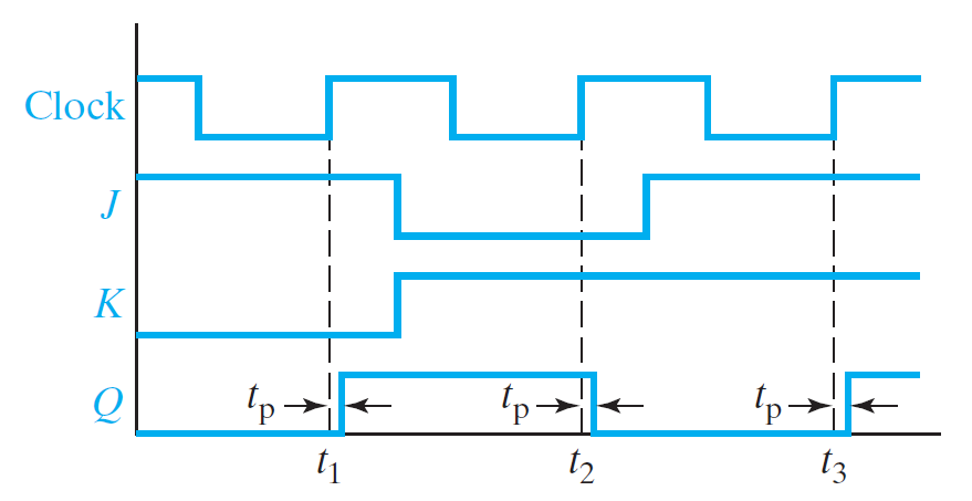
11.6 J-K Flip-Flop
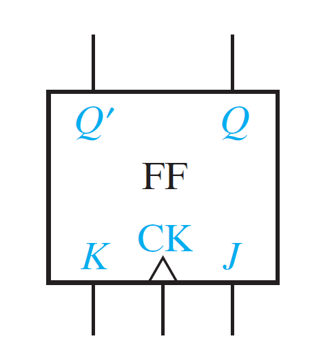
(rising-edge)

when Clk=1, ==P=JQ'+K'Q==
when J=K=1 and Clk=0→1, Q+=Q'
so ==J=K=1 is illegal==
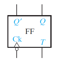
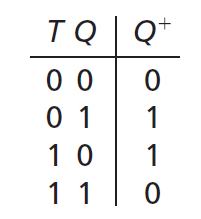
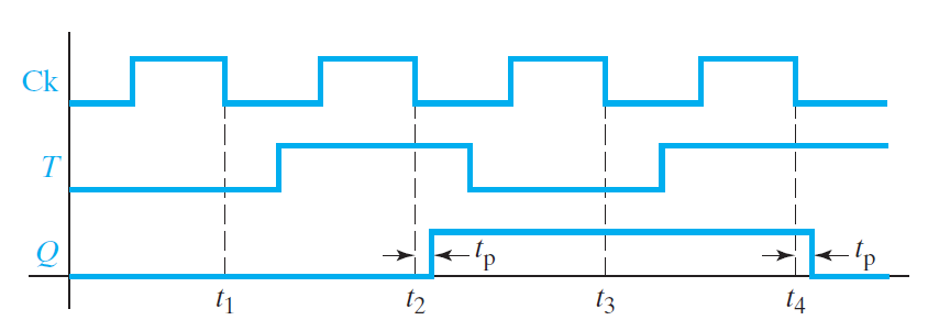
11.7 T Flip-Flop
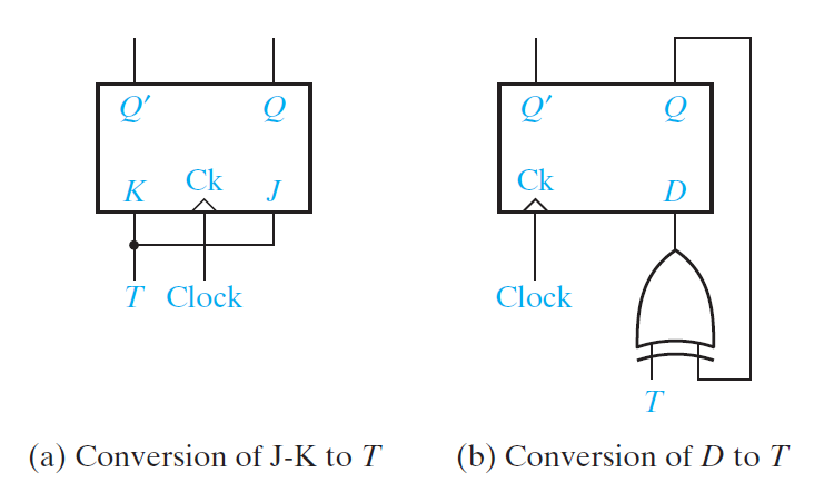
J-K flip-flop: Q+=JQ'+K'Q D flip-flop: Q+=D when Clk=1
==Q+ = TQ' + T'Q = T ⊕ Q==
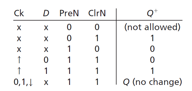
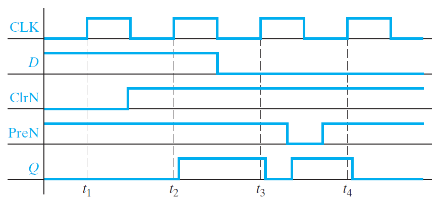
11.8 Flip-Flops with Additional Inputs
D flip-flop with clear and reset
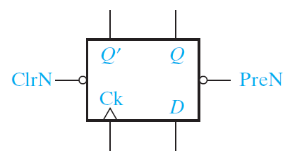 if ClrN=0 then Q→0
if PreN=0 then Q→1
D flip-flop with clock enable
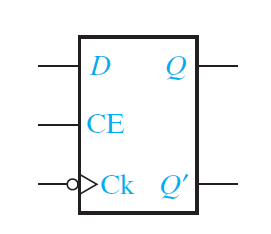
Q+ = Q·CE' + D·CE (when Ck=1)
implementation
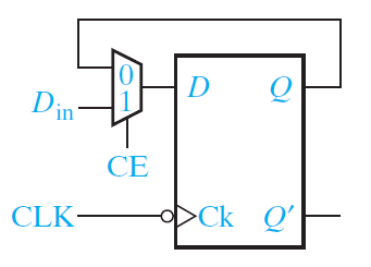
Q+ = Q·CE' + Din·CE
skip 11.9 =))
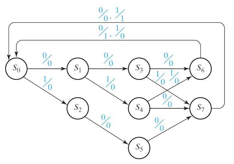
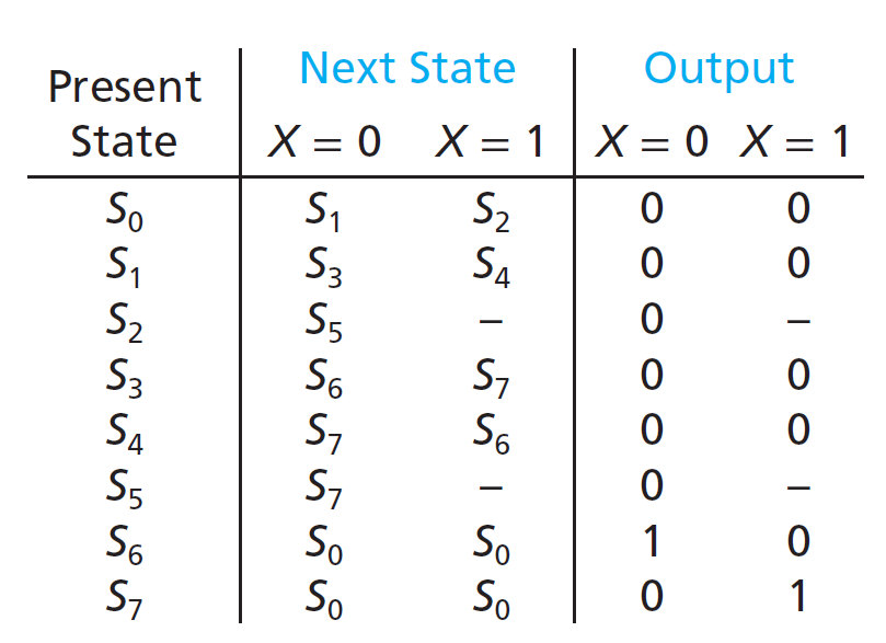
Ch14 Derivation of State Graphs and Tables
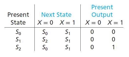
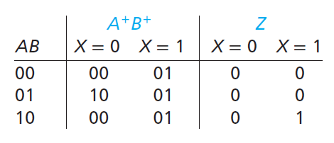
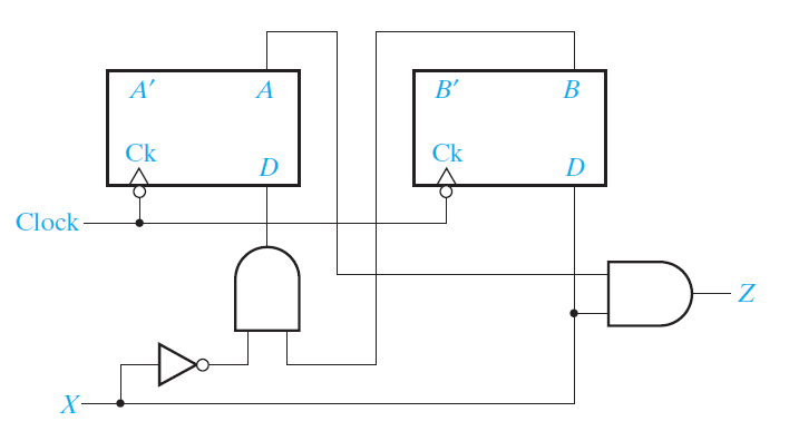
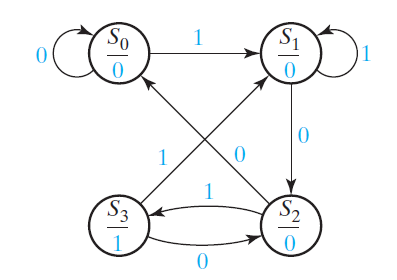
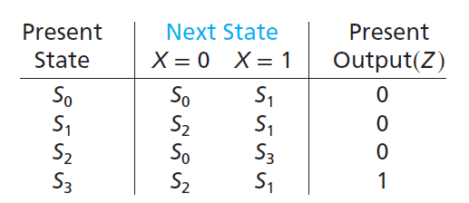
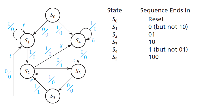
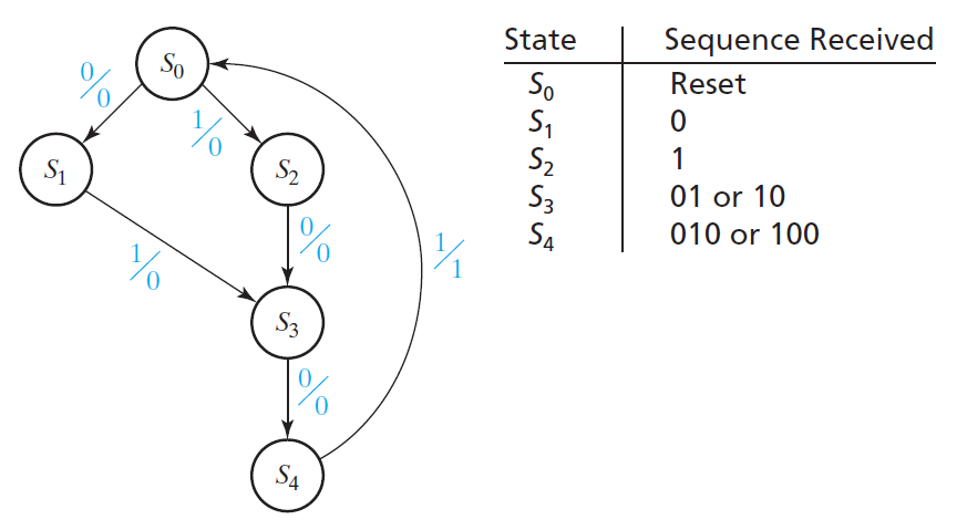
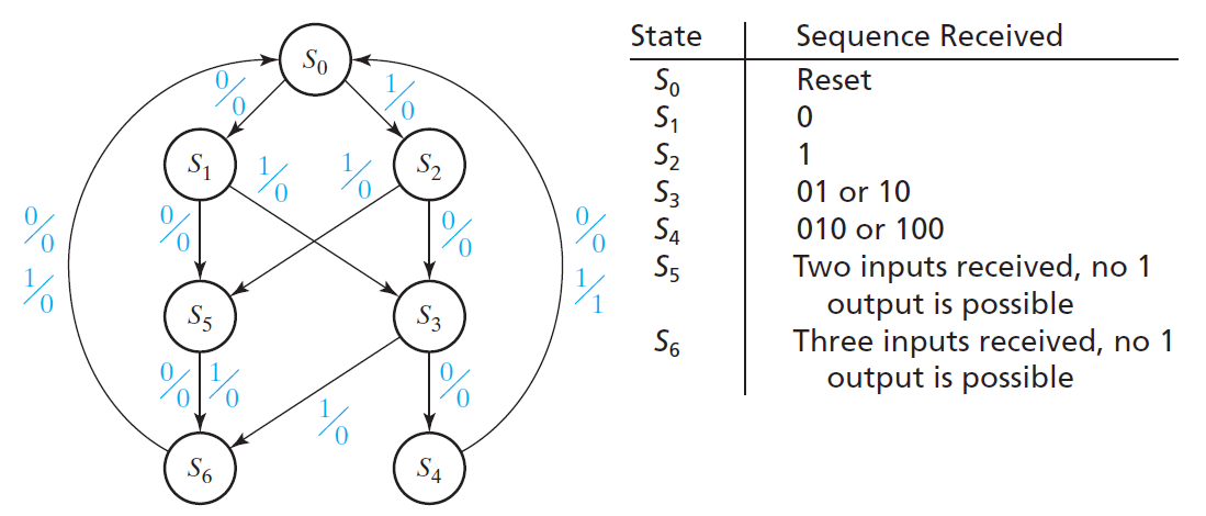
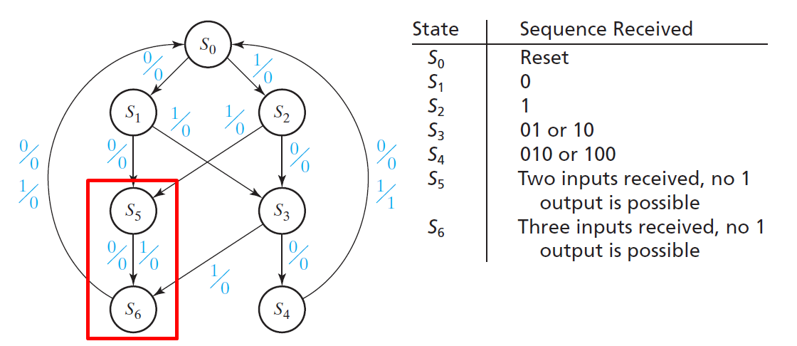
example:
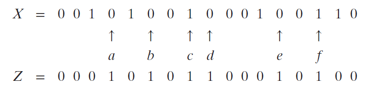
design the circuit so that any input sequence ending in 101 will produce an output Z = 1
coincident with the last 1
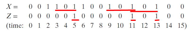 the symbol before the slash is the input and the symbol after the slash is the corresponding output
Mealy machine
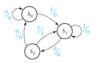
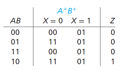
target: \(S_0S_1S_2\) = 101 \(S_0\): get 1 →store it ; get 0 → again
\(S_0S_1S_2\) 基本上可以隨便代
(i.e. \(S_0\) 可以 00 or 01 or whatever 代替)
出來的電路、SOP 會不一樣,但實質結果是相同的
Moore machine
initial state = 1
→ ++01++000 underline part Z=1
14.2 More Complex Design Problems
a Mealy example
The output Z should be 1 if the input sequence ends in either 010 or 1001, and Z should be 0 otherwise.
010| _10|01
1001| __ 01|0
"|": 接在一起處
a Moore example
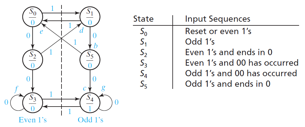
The output Z is to be 1 if the total number of 1’s received is ++odd++ and at least ++two consecutive 0s++ have been received.

14.3 Guidelines for Construction of State Graphs
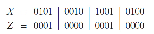
The circuit examines groups of four consecutive inputs and produces an output Z = 1 if the input sequence 0101 or 1001 occurs. The circuit resets after every four inputs.
【Mealy】
0101 & 1001 可共用
錯的 → 進到紅框區 → output 0
a group of 5 → 下面再多一層 以此類推
==跳過 example 2, 3==
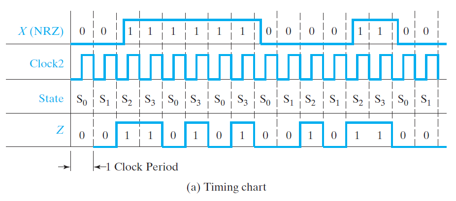
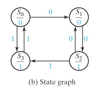
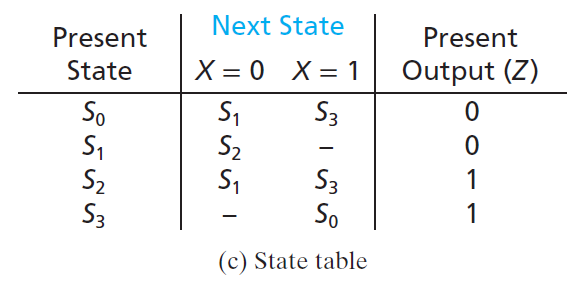
14.4 Serial Data Code Conversion
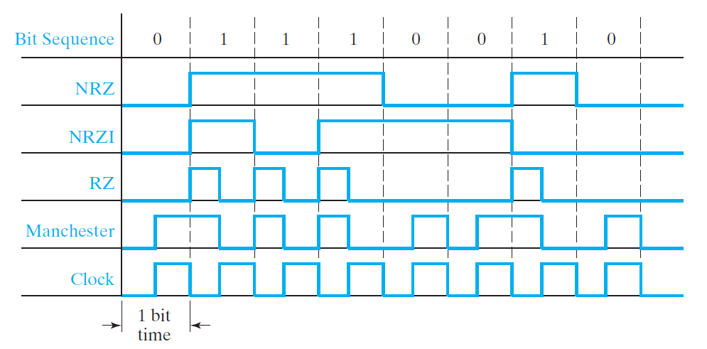
NRZ:non return to zero, 不變
RZ:return to 0, 變 1 後, 後半變回 0
NRZI:inverted, 看 1 的奇偶 (i.e. 0 → \(Q^+=Q\) ; 1 → \(Q^+=Q'\))
Manchester:0 → 後半變 1 ; 1 → 後半變 0
Mealy ver.
NRZ {→|convert} Manchester
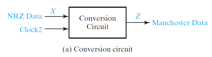
ideal:忽略延遲
actual:有延遲,出現 false output
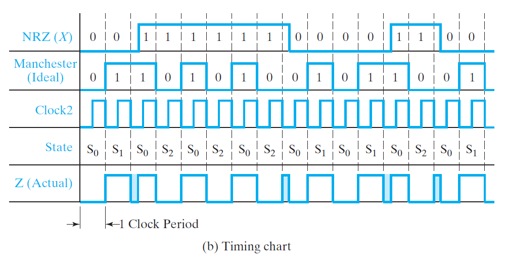
clock2 頻率 2 倍 → 所有 output changes 都在 edge 上
NRZ stable for 2 clock2 period
clock change but input hasn't → glitch
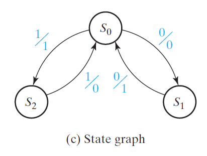
\(S_1\) 完不會有 1 so -
Moore ver.
NRZ {→|convert} Manchester
14.5 Alphanumeric State Graph Notation
(a) F → forward ; R → reverse
(b) 考量到 FR=11,00
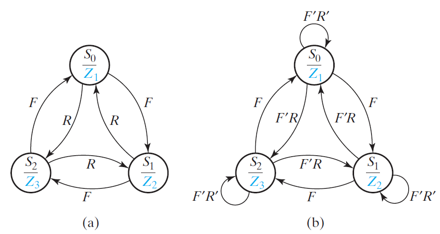
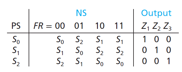
從 \(S_0\) 發出的線
3 條線 or 在一起,為 1 → 至少一條為 1
F + F′R + F′R′ = F + F′ = 1
3 條線兩兩 and 在一起,皆為 0 → 小於 2 條為 1
F·F′R = 0, F·F′R′ = 0, F′R·F′R′ = 0
→ 恰好 1 條為 1
for Mealy:
\(X_iX_j/Z_pZ_q\) means if \(X_iX_j\) = 11 (other Xs don't care), \(Z_pZ_q = 11\) (others Zs = 0)
e.g. \(X_1X_4'/Z_2Z_3\) means 1--0/0110
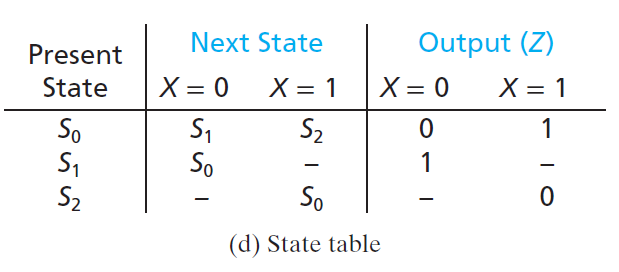
14.6 Incompletely Specified State Tables
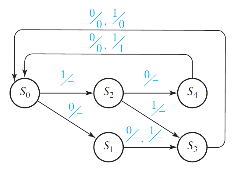
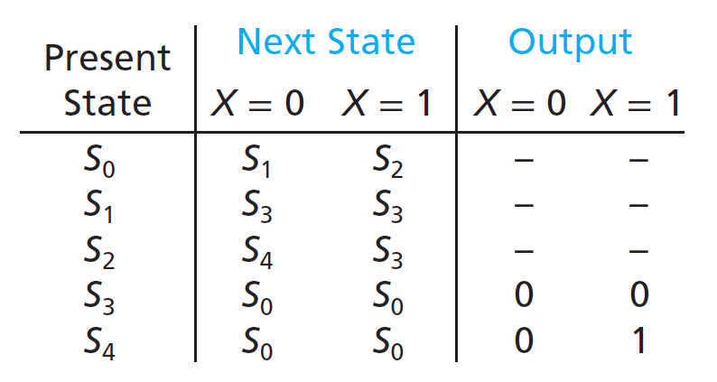
BCD (0~9 in binary i.e. 0000-1001)
while in last bit:
if 1s = even → 1
else → 0
101 disjoint, output only used in the end
Problems
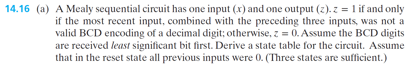
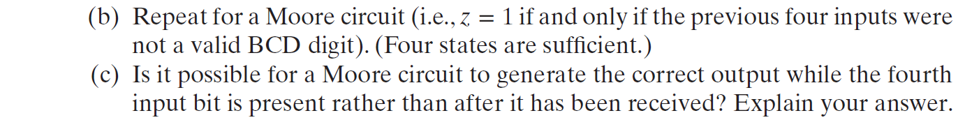
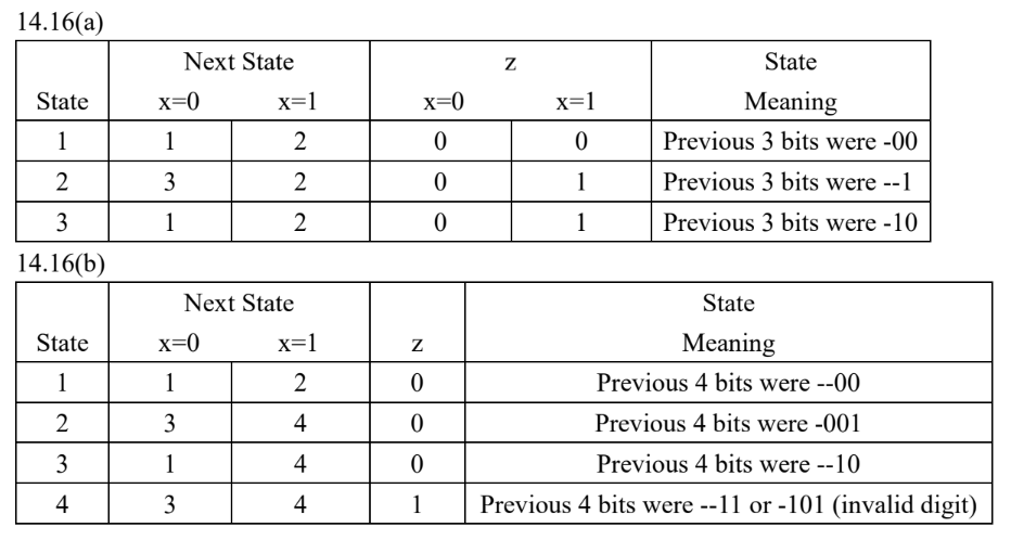
14.16
ans
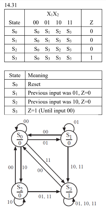
14.31

ans
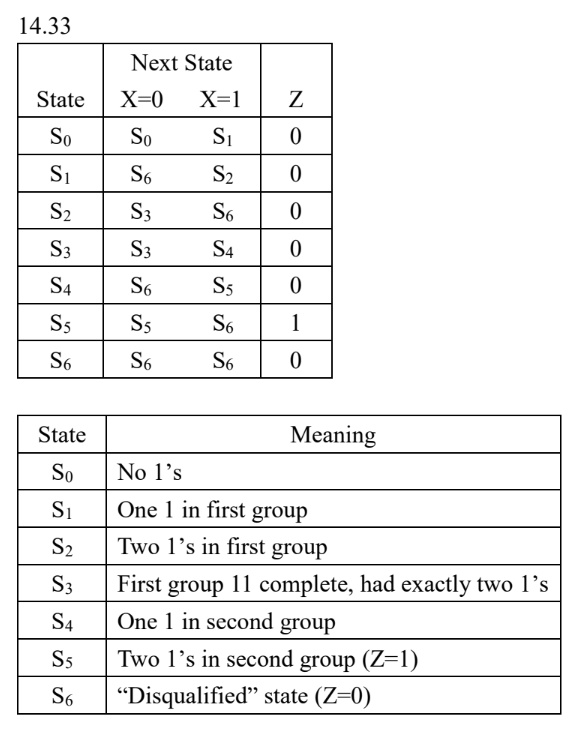
14.33
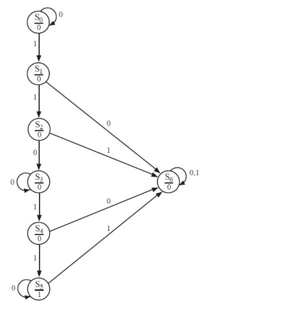
 ans
ans
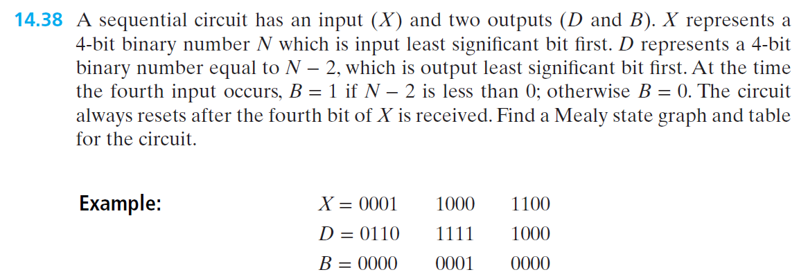
14.38
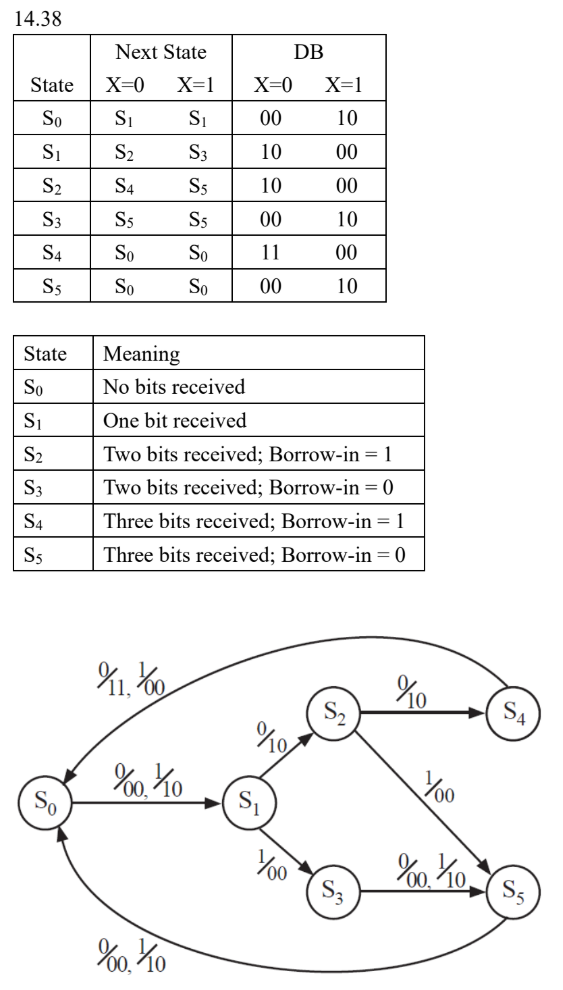
 ans
ans
14.43
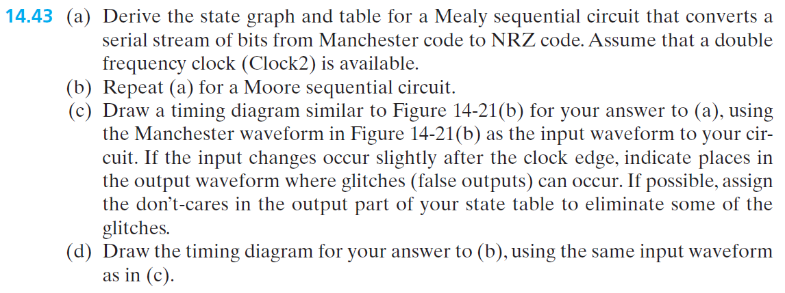 ans
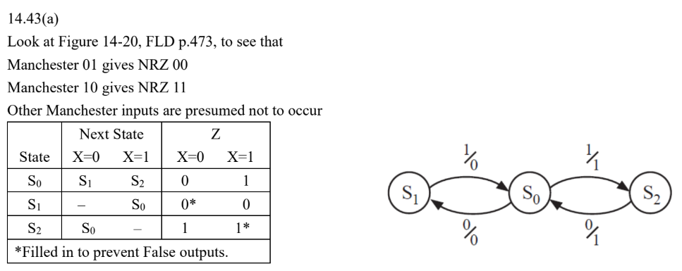
ans
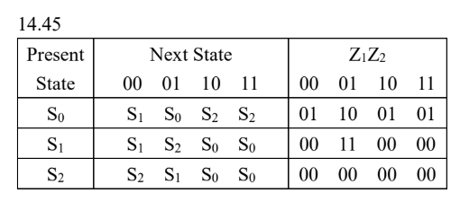
14.45
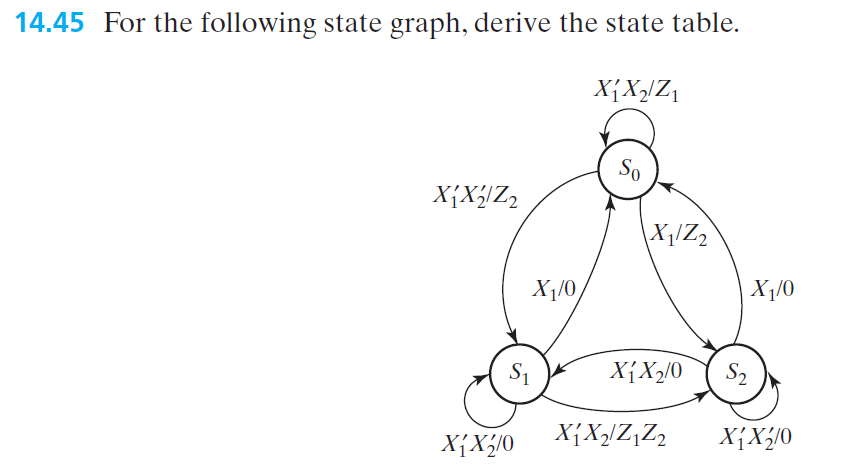 ans
ans